









































Technology ID
TT-0029
Description
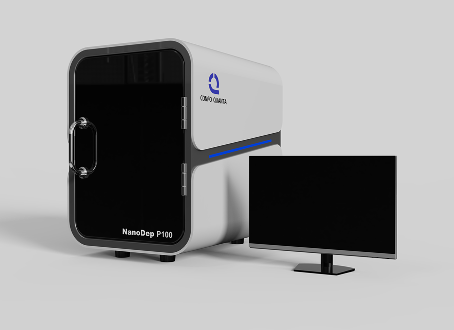
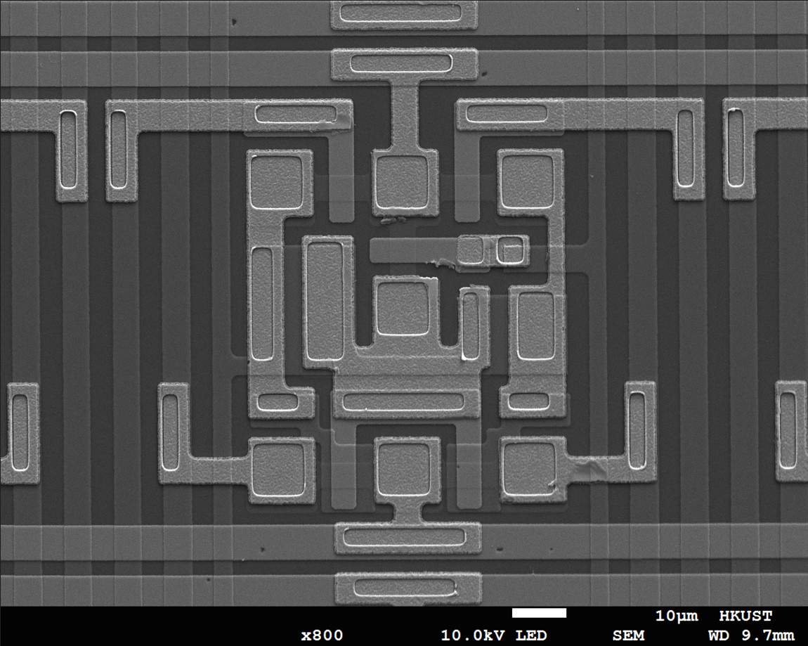
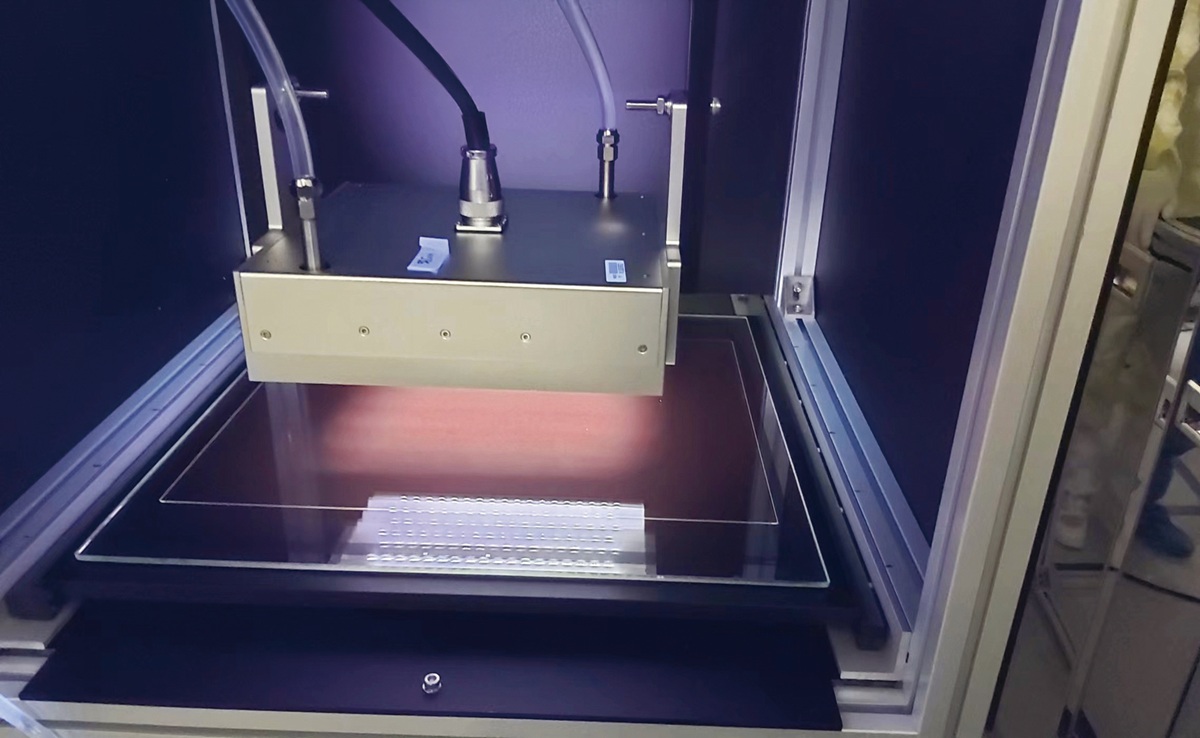
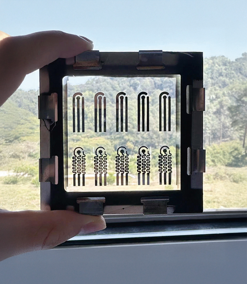
The photon induced material deposition method uses a focused laser to trigger local photo-catalysis reduction reactions and form patterned material. The technology enables additive manufacturing of electronics with nanoscale features on various substrates.
Content
Low cost, single-step, customized and fast additive manufacturing of functional material structures with nanoscale resolution and high performance
The deposition method applies to a wide range of conductor, insulator and semiconductor on various substrates, whether stiff or flexible, transparent or opaque
The material used for fabrication is environmentally friendly, nonhazardous and sustainable
Inventors
Applicable Industries
Potential Application
Technology Focus
TRL
Images